> ## Documentation Index
> Fetch the complete documentation index at: https://dragonwingdocs.qualcomm.com/llms.txt
> Use this file to discover all available pages before exploring further.
# PCIe
PCIe uses a bidirectional connection to send and receive information at the same time, as shown in the following figure.

Figure: PCIe device connection link
The path between the devices is called a Link. It is made up of one or more transmit and receive pairs. One pair of the Link is called a Lane. The PCIe device connection in Qualcomm Linux devices supports 16 lanes. The number of lanes or the Link width is x16.
The following table lists the types of PCIe connections for devices.
Table : PCIe connections
|
PCIe type
|
Description
|
|
Root complex (RC)
|
Connects the CPU to the PCIe topology
|
|
Switch
|
Connects more than 2 ports and acts as a packet router
|
|
Bridge
|
Connects different buses: for example, PCIe to PCIe, or PCIe to peripheral component interconnect (PCI)
|
|
Endpoint (EP)
|
Resides at the bottom of the PCIe topology tree structure and has only an upstream port
|
|
Legacy endpoint
|
Uses older PCI bus operations to support backward compatibility
|
## **PCIe host mode enumeration feature**
When a system first powers up, the configuration software running on the system host processor is aware of the existence of only Bus 0 (if PCIe is supported). The software is not aware of the bus topology or any device connected to the bus. The enumeration process discovers the various buses, devices, and functions present in the system.
When enumeration is complete, each bus in the system is numbered as follows:
* The primary bus number indicates the bus that directly connects to the primary interface of the bridge (towards the root complex).
* The secondary bus number indicates the bus that directly connects to the secondary interface of the bridge (away from the root complex).
* The subordinate bus number indicates the highest numbered bus that exists on the downstream side of the bridge.
The BDF number uniquely identifies each device. The ID-based routing method of the transaction layer packet (TLP) uses this number. The PCIe host mode enumeration process involves the following:
1. Link training
2. Scanning for devices on the bus
3. Registration
For more information on the PCIe device initialization, enumeration process, see [https://www.kernel.org/doc/html/latest/PCI/index.html](https://www.kernel.org/doc/html/latest/PCI/index.html).
## **PCIe layered architecture**
The following figure shows the PCIe software architecture.
Figure : PCIe software architecture
The following figure shows the layered architecture model of PCIe.

Figure : PCIe layered architecture
The transmission units exchanged are as follows.
* Ordered set between the physical layer entities.
* Data link layer packet (DLLP) between data link layer entities.
* Transaction layer packet (TLP) between transaction layer entities.
The following table lists the three layers, with the respective functions, in the PCIe architecture.
Table : Layers in PCIe architecture
|
Layer
|
Features
|
|
Physical layer
|
Logical sub-block: Link training, initialization, and maintenance.
|
|
Physical sub-block: 8b/10b encoding and decoding, and parallel-to-serial and serial-to-parallel conversion.
|
|
Data link layer
|
Assembly and disassembly of the DLLP packet.
|
|
Generation and validation of the link layer CRC (LCRC).
|
|
Acknowledgment and no acknowledgment protocol (replay of TLPs in error).
|
|
Transaction layer
|
Assembly and disassembly of the TLP packet.
|
|
Generation and validation of end-to-end CRC (ECRC).
|
|
Flow control receives entity advertises for the available receive buffer size information using DLLPs.
|
|
Quality of service (QoS): traffic class (TC) to virtual channel (VC) mapping.
|
|
Transaction ordering: implements the transaction ordering rule within a VC.
|
PCI defines a dedicated block of configuration address space for each function as shown in the following figure. The software determines the presence of a function, configures it, and checks and controls its status.

Figure : PCIe configuration address space
## **PCIe software driver configuration**
The PCIe controller driver initializes the PCIe resources and performs link training. After successful training, the controller driver calls the PCIe framework for link enumeration, such as endpoint discovery, identifying the client driver, and probing those drivers. For more information about the PCIe framework and client driver PCIe registrations, see [https://www.kernel.org/doc/html/latest/PCI/index.html](https://www.kernel.org/doc/html/latest/PCI/index.html).
### **Link training**
Link training comprises the following operations:
1. The PCIe driver `pcie-qcom.c` file at [https://github.com/torvalds/linux/blob/master/drivers/pci/controller/dwc/pcie-qcom.c](https://github.com/torvalds/linux/blob/master/drivers/pci/controller/dwc/pcie-qcom.c) obtains the required resources such as regulators, clocks, from the device tree.
2. The PCIe driver calls Synopsys DesignWare® Core host driver *pcie-designware-host.c* file at [https://github.com/torvalds/linux/blob/master/drivers/pci/controller/dwc/pcie-designware-host.c](https://github.com/torvalds/linux/blob/master/drivers/pci/controller/dwc/pcie-designware-host.c) to initialize the root complex.
3. The Synopsys DesignWare Core driver performs all necessary initializations.
4. The Synopsys DesignWare Core driver calls a function pointer to perform host initialization.
5. The Qualcomm PCIe driver performs PHY power-on, enables all regulators, clocks.
6. The Synopsys DesignWare Core driver starts the link training by calling the function pointer to start the link.
### **Hardware initialization**
The driver initializes and configures the PCIe hardware block and performs link training. The initialization occurs after the `platform _probe()` driver function is called.
```bash theme={null}
static int qcom_pcie_probe(struct platform_device *pdev)
{
// get PCIe resources
ret = dw_pcie_host_init(pp); // call DWC framework to host intialisation like MSI, MSIx and controller init
if (ret) {
dev_err(dev, "cannot initialize host\n");
goto err_phy_exit;
}
};
static const struct of_device_id qcom_pcie_match[] = {
{ .compatible = "qcom,pcie-sc7280", .data = &cfg_1_9_0 },
{}
};
static struct platform_driver qcom_pcie_driver = {
.probe = qcom_pcie_probe,
.driver = {
.name = "qcom-pcie",
.suppress_bind_attrs = true,
.of_match_table = qcom_pcie_match,
},
};
```
When the Synopsys DesignWare Core driver is initialized, it also initializes MSI, MSIx, and controllers. The driver calls a Qualcomm function pointer to start the link training.
```bash theme={null}
static int qcom_pcie_start_link(struct dw_pcie *pci)
{
struct qcom_pcie *pcie = to_qcom_pcie(pci);
/* Enable Link Training state machine */
if (pcie->cfg->ops->ltssm_enable)
pcie->cfg->ops->ltssm_enable(pcie);
return 0;
}
static int qcom_pcie_link_up(struct dw_pcie *pci)
{
u16 offset = dw_pcie_find_capability(pci, PCI_CAP_ID_EXP);
u16 val = readw(pci->dbi_base + offset + PCI_EXP_LNKSTA);
return !!(val & PCI_EXP_LNKSTA_DLLLA); // checks the link is up or not
}
static const struct dw_pcie_ops dw_pcie_ops = {
.link_up = qcom_pcie_link_up,
.start_link = qcom_pcie_start_link,
};
```
The Synopsys DesignWare Core driver waits for the link to be active to enumerate the PCI framework. The Qualcomm PCIe driver enables only the link training.
Note: The PCIE\_0 root complex instance is enabled by default for the WLAN EP connection.
## Enable QPS615 PCIe switch
This section describes how to enable a QPS615 PCIe switch in the Qualcomm Linux hardware SoCs. The QPS615 switch endpoint is supported on the `PCIe1` instance. The following figure shows the QPS615 endpoint and connections.

Figure : QPS615 PCIe switch connection diagram
The Qualcomm PCIe driver documentation can be accessed at the following locations:
* [https://github.com/torvalds/linux/blob/master/Documentation/devicetree/bindings/pci/qcom%2Cpcie-sc8280xp.yaml](https://github.com/torvalds/linux/blob/master/Documentation/devicetree/bindings/pci/qcom%2Cpcie-sc8280xp.yaml)
* [https://elixir.bootlin.com/linux/v6.6.48/source/Documentation/devicetree/bindings/pci/qcom,pcie.yaml](https://elixir.bootlin.com/linux/v6.6.48/source/Documentation/devicetree/bindings/pci/qcom,pcie.yaml)
* [https://github.com/torvalds/linux/blob/master/Documentation/devicetree/bindings/phy/qcom%2Csc8280xp-qmp-pcie-phy.yaml](https://github.com/torvalds/linux/blob/master/Documentation/devicetree/bindings/phy/qcom%2Csc8280xp-qmp-pcie-phy.yaml)
### **PCIe-related configurations**
The following configurations are enabled by default to support the QPS615 switch. Disable the QPS615 switch default support, by reverting the code changes, to use it for a different PCIe endpoint.
To enable PCIe-related `configs`, apply the following patch to the */arch/arm64/configs/qcom\_addons.config* file.
```bash theme={null}
QCLINUX: arm64: defconfig: qcom:
diff --git a/arch/arm64/configs/qcom_defconfig b/arch/arm64/configs/qcom_defconfig
index 7293680..730122c 100644
--- a/arch/arm64/configs/qcom_defconfig
+++ b/arch/arm64/configs/qcom_defconfig
@@ -173,6 +173,7 @@
CONFIG_HOTPLUG_PCI=y
CONFIG_HOTPLUG_PCI_ACPI=y
CONFIG_PCI_HOST_GENERIC=y
+CONFIG_PCIE_DW_PLAT_HOST=y
CONFIG_PCIE_QCOM=y
CONFIG_PCI_ENDPOINT=y
CONFIG_PCI_ENDPOINT_CONFIGFS=y
@@ -793,3 +794,5 @@
CONFIG_CORESIGHT_TPDM=m
CONFIG_CORESIGHT_DUMMY=m
CONFIG_MEMTEST=y
+CONFIG_PCIEASPM=y
+CONFIG_PCIEASPM_POWER_SUPERSAVE=y
```
### **Message signaled interrupt (MSI)**
The current MSI mapping doesn't have all the vectors. The Qualcomm Linux hardware SoCs support eight vectors. Each vector in turn supports 32 MSIs. Therefore, the total MSIs supported are 256.
For information about adding all the MSI groups supported for this PCIe instance, see [https://lore.kernel.org/linux-arm-msm/f1168212-bc6e-4570-869c-2870d6f248ad@linaro.org/T/](https://lore.kernel.org/linux-arm-msm/f1168212-bc6e-4570-869c-2870d6f248ad@linaro.org/T/).
### **Sample PCIe kernel driver log**
The following is a sample PCIe kernel driver log from the QPS615 device enumeration.
    {`[    7.254674] qcom-pcie 1c08000.pci: supply vdda not found, using dummy regulator
        [    7.285224] qcom-pcie 1c08000.pci: supply vddpe-3v3 not found, using dummy regulator
        [    7.299688] qcom-pcie 1c08000.pci: host bridge /soc@0/pci@1c08000 ranges:
        [    7.313713] qcom-pcie 1c08000.pci: IO 0x0040200000..0x00402fffff -> 0x0000000000
        [    7.329778] qcom-pcie 1c08000.pci: MEM 0x0040300000..0x005fffffff -> 0x0040300000
        [    7.479174] qcom-pcie 1c08000.pci: iATU: unroll T, 8 ob, 8 ib, align 4K, limit 1024G
        [    7.577792] qcom-pcie 1c08000.pci: PCIe Gen.3 x2 link up
        [    7.648353] qcom-pcie 1c08000.pci: PCI host bridge to bus 0001:00
        [    7.654618] pci_bus 0001:00: root bus resource [bus 00-ff]
        [    7.654620] pci_bus 0001:00: root bus resource [io  0x0000-0xfffff]
        [    7.654622] pci_bus 0001:00: root bus resource [mem 0x40300000-0x5fffffff]
        [    7.654633] pci 0001:00:00.0: [17cb:010b] type 01 class 0x060400
        [    7.665893] pci 0001:00:00.0: reg 0x10: [mem 0x00000000-0x00000fff]
        [    7.684913] pci 0001:00:00.0: PME# supported from D0 D3hot D3cold
        [    7.700502] pci 0001:01:00.0: [1179:0623] type 01 class 0x060400
        [    7.710817] pci 0001:01:00.0: PME# supported from D0 D3hot D3cold
        [    7.733698] pci 0001:01:00.0: bridge configuration invalid ([bus 00-00]), reconfiguring
        [    7.738818] pci 0001:02:01.0: [1179:0623] type 01 class 0x060400
        [    7.751157] pci 0001:02:01.0: PME# supported from D0 D3hot D3cold
        [    7.763174] pci 0001:02:02.0: [1179:0623] type 01 class 0x060400
        [    7.777084] pci 0001:02:02.0: PME# supported from D0 D3hot D3cold
        [    7.792832] pci 0001:02:03.0: [1179:0623] type 01 class 0x060400
        [    7.815659] pci 0001:02:03.0: PME# supported from D0 D3hot D3cold`}
## **Ethernet interfaces supported through QPS615 PCIe switch**
The QPS615 PCIe switch enables Ethernet connectivity for the device. When the device loads the QPS615 driver and establishes the PCIe link, it automatically activates the supported Ethernet interfaces, by default, during device startup.
To customize the default configuration or enable extra MAC/PHY components beyond Qualcomm’s hardware setup, see the *Bring up Ethernet* section in the [*Qualcomm Linux Ethernet guide*](https://docs.qualcomm.com/bundle/publicresource/topics/80-80021-26/bring_up-ethernet.html).
Table : Supported Ethernet interfaces
|
Interface type
|
Speed
|
Connector type
|
Description
|
|
QEP PHY (SGMII)
|
2.5 GbE
|
IX/RJ45 connector (QEP8121)
|
|
|
AQR PHY (USXGMII)
|
10 GbE
|
IX/RJ45 connector (AQR113C)
|
-
The 10 Gigabit Ethernet AQR PHY is an optional component in the RB3 Gen 2 Development Kit,
and the Evaluation Kits (EVK) for Dragonwing IQ-8275 and Dragonwing IQ-9075.
It’s validated on AQR113C.
|
### **Bring up alternate hardware components**
You can attach MAC/PHY components other than the hardware configuration provided by Qualcomm and bring them up.
To replace QPS615 with other PCIe based MAC/PHY, see [Enable QPS615 PCIe switch](#enable-qps615-pcie-switch).
Note: You must obtain the MAC/PHY driver and firmware from the respective vendor. Qualcomm isn’t responsible for these configuration changes.
## **Enable USB interface through PCIe switch**
This section provides instructions on how to activate a USB interface through a PCIe switch in the Qualcomm Linux hardware SoCs. The PCIE1 instance is connected to the endpoint of the QPS615 switch, and the downstream port of the QPS615 is connected to the PCIe to USB endpoint. For the PCIe to USB endpoint connections using the QPS615, see the mainboard and interposer block diagram at [https://docs.qualcomm.com/bundle/publicresource/topics/80-80021-251/rb3\_hardware\_overview.html](https://docs.qualcomm.com/bundle/publicresource/topics/80-80021-251/rb3_hardware_overview.html).
Note: Dragonwing IQ-9075 PCIe software doesn't support USB.
Power to usb hub is enabled through pwrctrl driver, Please refer below upstream links for these details.
[https://elixir.bootlin.com/linux/v7.1/source/arch/arm64/boot/dts/qcom/qcs6490-rb3gen2.dts#L896](https://elixir.bootlin.com/linux/v7.1/source/arch/arm64/boot/dts/qcom/qcs6490-rb3gen2.dts#L896)
[https://elixir.bootlin.com/linux/v7.1/source/Documentation/devicetree/bindings/usb/renesas,upd720201-pci.yaml](https://elixir.bootlin.com/linux/v7.1/source/Documentation/devicetree/bindings/usb/renesas,upd720201-pci.yaml)
[https://elixir.bootlin.com/linux/v7.1/source/drivers/pci/pwrctrl/generic.c](https://elixir.bootlin.com/linux/v7.1/source/drivers/pci/pwrctrl/generic.c)
````
### **Avoid early handoff in PCIe to USB controller**
Ensure that `usb_early-handoff` is skipped for the PCIe to USB controller since the firmware isn't loaded. This precaution is necessary to prevent any adverse impact on the bootup duration.
```text
diff --git a/drivers/usb/host/pci-quirks.c b/drivers/usb/host/pci-quirks.c
index 2665832..c3d488f 100644
--- a/drivers/usb/host/pci-quirks.c
+++ b/drivers/usb/host/pci-quirks.c
@@ -1260,6 +1260,11 @@
return;
}
+ /* Skip handoff for Renesas PCI USB controller on QCOM SOC */
+ if ((pdev->vendor == PCI_VENDOR_ID_RENESAS) &&
+ (pcie_find_root_port(pdev)->vendor == PCI_VENDOR_ID_QCOM))
+ return;
+
if (pdev->class != PCI_CLASS_SERIAL_USB_UHCI &&
pdev->class != PCI_CLASS_SERIAL_USB_OHCI &&
pdev->class != PCI_CLASS_SERIAL_USB_EHCI &&
````
### **Download PCIe to USB controller firmware**
To download the firmware from [https://www.renesas.com/us/en/products/interface/usb-switches-hubs/upd720201-usb-30-host-controller#design\_development](https://www.renesas.com/us/en/products/interface/usb-switches-hubs/upd720201-usb-30-host-controller#design_development), register and log in to [https://www.renesas.com/](https://www.renesas.com/). Rename the downloaded firmware file to *renesas\_usb\_fw\.mem*.
Note: To prevent command failures, update the software as described in the [Set up the device](https://docs.qualcomm.com/bundle/publicresource/topics/80-80021-251/set_up_the_device.html) section before updating the Renesas firmware.
Option 1 (Ubuntu): Push the firmware files using SCP or similar tools. For example,
```text theme={null}
scp renesas_usb_fw.mem root@10.92.175.138:/lib/firmware
```
Option 2 (Yocto):
1. Connect device to Host PC via USB cable for adb.
2. Push firmware to device.
```text theme={null}
mount -o remount,rw /usr
adb push renesas_usb_fw.mem /lib/firmware
```
3. To activate the firmware do either of the following options.
* Option A: Reboot target for USB type A ports.
* Option B: Manually bind the Renesas xHCI driver.
```text theme={null}
echo "0001:04:00.0" > /sys/bus/pci/drivers/xhci-pci-renesas/bind
```
4. Verify firmware enumeration.
```text theme={null}
dmesg
```
### **PCIe kernel driver logs for PCIe to USB device enumeration reference**
You can run the following commands to view the device information:
* To display device information in USB, run the following command.
```text theme={null}
lsusb
```
The following message is displayed.
```text theme={null}
Bus 002 Device 003: ID 0b95:1790 ASIX Electronics Corp. AX88179 Gigabit Ethernet
Bus 002 Device 002: ID 05e3:0625 Genesys Logic, Inc. USB3.2 Hub
Bus 002 Device 001: ID 1d6b:0003 Linux Foundation 3.0 root hub
Bus 001 Device 002: ID 05e3:0610 Genesys Logic, Inc. Hub
Bus 001 Device 001: ID 1d6b:0002 Linux Foundation 2.0 root hub
```
* To display device information in PCIe, run the following command.
```text theme={null}
lspci
```
The following message is displayed.
```text theme={null}
0001:00:00.0 PCI bridge: Qualcomm Device 010b
0001:01:00.0 PCI bridge: Toshiba Corporation Device 0623
0001:02:01.0 PCI bridge: Toshiba Corporation Device 0623
0001:02:02.0 PCI bridge: Toshiba Corporation Device 0623
0001:02:03.0 PCI bridge: Toshiba Corporation Device 0623
0001:04:00.0 USB controller: Renesas Technology Corp. uPD720201 USB 3.0 Host Controller (rev 03)
0001:05:00.0 Ethernet controller: Toshiba Corporation Device 0220
0001:05:00.1 Ethernet controller: Toshiba Corporation Device 0220
```
## **Connect QPS615 switches in cascade**
Connect the QPS615 switches in cascade to enable additional Ethernet, PCIe, and USB ports.
Note: This feature is supported only in QCS6490.
The following image shows the two QPS615 switches connected in cascade to PCIE1 and another QPS615 switch connected to PCIE2.
 To initiate the link training and enumeration for all endpoints, do the following:
1. To reset the QPS615 switch, toggle the RESX GPIOs for both QPS615 #1 and QPS615 #2.
2. To control the endpoint reset, trigger PERST. Both the switches share the PERST.
The devices can be attached directly to the QPS615 switch. The PCIe RC0 is attached to the WLAN endpoint. The following differences are due to the PCIe node hierarchy.
* Switch-attached devices:
* The QPS615 PCIe tree node hierarchy is statically fixed.
* All nodes for switching USP and DSP ports are created during PCIe initialization.
* One of the switch DSP ports represents WLAN.
* If you disable the WLAN node, it disables the WLAN device, but the PCIe downstream port remains enabled and returns a default maximum link width.
* Directly-attached WLAN devices:
* Disables only a single node.
* Returns the Invalid argument, when WLAN is disabled.
## **Enable NVMe through PCIe interface**
This section describes how to enable NVMe using PCIe for storage expansion. To verify if NVMe is connected over a PCIe interface, do the following:
1. To display PCIe device information, run the following command.
```text theme={null}
lspci
```
Output:
```text theme={null}
0000:00:00.0 PCI bridge: Qualcomm Device 0115
0000:01:00.0 Network controller: Qualcomm QCNFA765 Wireless Network Adapter (rev 01)
0001:00:00.0 PCI bridge: Qualcomm Device 0115
0001:01:00.0 Non-Volatile memory controller: Samsung Electronics Co Ltd NVMe SSD Controller PM9A1/PM9A3/980PRO
```
2. Locate the PCIe logs.
```text theme={null}
dmesg | grep pcie
```
Output:
```text theme={null}
[ 0.000000] Kernel command line: root=/dev/disk/by-partlabel/system rw rootwait console=ttyMSM0,115200n8
pcie_pme=nomsi net.ifnames=0 pci=noaer kpti=off kasan=off kasan.stacktrace=off swiotlb=128 earlycon reboot=panic_warm page_owner=on qcom_scm.download_mode=1 slub_debug=FZP,
zs_handle,zspage;FZPU mitigations=auto kernel.sched_pelt_multiplier=4 rcupdate.rcu_expedited=1 rcu_nocbs=0-7 no-steal-acc vfio_iommu_type1.allow_unsafe_interrupts=1 fw_devlink.strict=1
[ 3.842071] qcom-pcie 1c00000.pci: supply vdda not found, using dummy regulator
[ 3.845339] qcom-pcie 1c10000.pci: supply vdda not found, using dummy regulator
[ 3.845428] qcom-pcie 1c10000.pci: supply vddpe-3v3 not found, using dummy regulator
[ 3.845508] qcom-pcie 1c10000.pci: host bridge /pci@1c10000 ranges:
[ 3.845519] qcom-pcie 1c10000.pci: IO 0x0060200000..0x00602fffff -> 0x0000000000
[ 3.845526] qcom-pcie 1c10000.pci: MEM 0x0060300000..0x007fffffff -> 0x0060300000
[ 3.848154] qcom-pcie 1c00000.pci: supply vddpe-3v3 not found, using dummy regulator
[ 3.854556] qcom-pcie 1c00000.pci: host bridge /pci@1c00000 ranges:
[ 3.860574] qcom-pcie 1c00000.pci: IO 0x0040200000..0x00402fffff -> 0x0000000000
[ 3.867362] qcom-pcie 1c00000.pci: MEM 0x0040300000..0x005fffffff -> 0x0040300000
[ 3.963275] qcom-pcie 1c10000.pci: iATU: unroll T, 32 ob, 8 ib, align 4K, limit 1024G
[ 3.990385] qcom-pcie 1c00000.pci: iATU: unroll T, 32 ob, 8 ib, align 4K, limit 1024G
[ 4.072091] qcom-pcie 1c10000.pci: PCIe Gen.4 x2 link up
[ 4.080241] qcom-pcie 1c10000.pci: PCI host bridge to bus 0001:00
[ 4.291824] pcieport 0001:00:00.0: Adding to iommu group 9
[ 4.551677] pcieport 0001:00:00.0: PME: Signaling with IRQ 256
[ 4.572484] WARNING: CPU: 3 PID: 89 at drivers/pci/controller/dwc/pcie-qcom.c:1430 qcom_pcie_icc_update+0xf8/0x144
[ 4.595291] pc : qcom_pcie_icc_update+0xf8/0x144
[ 4.595293] lr : qcom_pcie_icc_update+0x9c/0x144
[ 4.640742] qcom_pcie_icc_update+0xf8/0x144
[ 4.640745] qcom_pcie_probe+0x234/0x30c
[ 4.988519] qcom-pcie 1c00000.pci: Phy link never came up
[ 5.302179] qcom-pcie 1c00000.pci: PCI host bridge to bus 0000:00
[ 5.372008] pcieport 0000:00:00.0: Adding to iommu group 10
[ 5.378905] pcieport 0000:00:00.0: PME: Signaling with IRQ 257
[ 11.564590] pcieport 0000:00:00.0: BAR 14: assigned [mem 0x40400000-0x405fffff]
```
3. To locate the NVMe directories, run the following command.
```text theme={null}
ls -lh /dev/nvme*
```
Output:
```text theme={null}
crw-------. 1 root root 508, 0 Jan 1 00:00 /dev/nvme0
brw-rw----. 1 root disk 259, 30 Jan 1 00:00 /dev/nvme0n1
```
## **PCIe client driver sample**
The client driver defines the `device-id` table and `pci_driver` structures, and registers with the PCIe framework. The following are a few PCIe client driver samples for reference.
* Sample data structure to hold client-specific private data.
```bash theme={null}
struct sample_driver_data {
int driver_data;
};
```
* Sample driver: You can provide data according to your driver-specific data structure.
```bash theme={null}
struct sample_driver_data info = {};
```
* Sample device ID table with the driver-specific data. The client driver registers with the `0x306` device ID.
```bash theme={null}
static const struct pci_device_id sample_pci_id_table[] = {
{ PCI_DEVICE_SUB(PCI_VENDOR_ID_QCOM, 0x0306, PCI_VENDOR_ID_QCOM, 0x010c),
.driver_data = (kernel_ulong_t) &info },
{ }
};
MODULE_DEVICE_TABLE(pci, sample_pci_id_table);
```
Note: `MODULE_DEVICE_TABLE(pci, sample_pci_id_table);` is mandatory.
* Sample `pci_driver` data structure with client driver name, `pci-id` table, and callbacks. The pointer to this structure is passed while registering with the PCI frame work.
```bash theme={null}
static struct pci_driver sample_pci_driver = {
.name = "Sample-PCI-Client-driver", /* Give the name that suites your driver description */
.id_table = sample_pci_id_table, /* pci core driver will compare from ids's supplied in this table with the enumerated endpoints */
.probe = sample_pci_probe, /* probe function is invoked by the PCI f/w when id matches with the endpoint id's */
.remove = sample_pci_remove, /* Remove function is invoked by PCI f/w when senses the attached endpoint/function is detached or down */
.driver.pm = &sample_pci_pm_ops /* pm ops that will be called from the pci core driver*/
};
```
* To register with PCI firmware, call `pci_register_driver(&sample_pci_driver)` from `module_init()`.
```bash theme={null}
module_pci_driver(sample_pci_driver);
```
## **PCIe bringup**
For information about PCIe bringup, see [PCIe-related configurations](https://docs.qualcomm.com/doc/80-80021-8/topic/pcie.html?product=895724676033554725\&facet=Interfaces\&version=2.0-rc2#pcie-software-support-feature-for-qps615__section_xbl_hhd_l1c) and [QPS615 switch support](https://docs.qualcomm.com/doc/80-80021-8/topic/pcie.html?product=895724676033554725\&facet=Interfaces\&version=2.0-rc2#pcie-software-support-feature-for-qps615__section_nmw_5jd_l1c).
## **PCIe power optimization**
PCIe defines two types of power management methods.
* Power management software that determines the power management capability of each device and manages each device individually
* System that doesn't require software intervention such as active state power management (ASPM)
During a time period when no packet is transmitted through the link, a device places the link into a power-saving state.
### **PCIe L0 link states**
PCIe power management defines the following L0 link states:
* L0: active state where all PCIe transactions and other operations are enabled
* L0s: ASPM state with low-resume latency (energy saving standby state)
### **PCIe device states**
PCIe power management defines the following device states:
* D0 (mandatory): The device is in full ON state, where there are two substates
* D0uninitialized: The function is present in the D0uninitialized state after the device comes out of reset, waiting to be enumerated and configured.
* D0active
* The function is present in the D0active state following the completion of the enumeration and configuration process.
* The function enters the D0active state when the system software enables one or more (in any combination) function parameters, such as memory space enable, I/O space enable, or BME bits.
* D1 (optional): light-sleep state
* The function can't initiate a TLP except for the PME message
* The function can't act as the target of transactions other than for configuration transactions.
* The function issues a software command to enter the D1 state by programming the PM control and status register.
* D2 (optional): deep-sleep state
* The function can't initiate a TLP except for the PME message
* The function can't act as the target of transactions other than configuration transactions.
* The function issues a software command to enter the D2 state by programming the PM control and status register.
* D3 (mandatory): device is the lowest power state, where the function must support both the D3 states
* D3hot
* The function can't initiate a TLP except for the PME message.
* The function can't act as the target of transactions other than configuration transactions.
* The function issues a software command to enter the D3hot state by programming the power state field.
* D3cold: device enters the D3cold state and power is removed; when power is restored, the device enters the D0uninitialized state.
## **PCIe verification**
For information about PCIe verification, see [PCIe-related configurations](https://docs.qualcomm.com/doc/80-80021-8/topic/pcie.html?product=895724676033554725\&facet=Interfaces\&version=2.0-rc2#pcie-software-support-feature-for-qps615__section_xbl_hhd_l1c) and [QPS615 switch support](https://docs.qualcomm.com/doc/80-80021-8/topic/pcie.html?product=895724676033554725\&facet=Interfaces\&version=2.0-rc2#pcie-software-support-feature-for-qps615__section_nmw_5jd_l1c).
## **Debug PCIe issues**
The `lspci` and `setpci` commands are native to Linux distributions. These commands have various levels of output. These commands also provide a useful point-in-time look at the capabilities and status of the different components trained on the PCI bus. Most of these capabilities are reflections of the configuration space registers required by the PCIe base specification. For more details, see [https://pcisig.com/specifications](https://pcisig.com/specifications). To view the usage instructions, run the following command.
```text theme={null}
lspci --help
```
The following features are useful in troubleshooting PCIe issues.
* Display device information
```text theme={null}
lspci
```
The following message is displayed.
```text theme={null}
0001:00:00.0 PCI bridge: Qualcomm Device 010b
0001:01:00.0 PCI bridge: Toshiba Corporation Device 0623
0001:02:01.0 PCI bridge: Toshiba Corporation Device 0623
0001:02:02.0 PCI bridge: Toshiba Corporation Device 0623
0001:02:03.0 PCI bridge: Toshiba Corporation Device 0623
0001:04:00.0 USB controller: Renesas Technology Corp. uPD720201 USB 3.0 Host Controller (rev 03)
0001:05:00.0 Ethernet controller: Toshiba Corporation Device 0220
0001:05:00.1 Ethernet controller: Toshiba Corporation Device 0220
```
* Display PCIe device and vendor IDs in the device control register.
```text theme={null}
lspci -nvmm
```
The following message is displayed.
```text theme={null}
Slot: 0001:00:00.0
Class: 0604
Vendor: 17cb
Device: 010b
DTNode: /sys/firmware/devicetree/base/soc@0/pci@1c08000/pcie@0
IOMMUGroup: 33
Slot: 0001:01:00.0
Class: 0604
Vendor: 1179
Device: 0623
DTNode: /sys/firmware/devicetree/base/soc@0/pci@1c08000/pcie@0/pcie1_bus1_dev0_fn0
IOMMUGroup: 33
Slot: 0001:02:01.0
Class: 0604
Vendor: 1179
Device: 0623
DTNode: /sys/firmware/devicetree/base/soc@0/pci@1c08000/pcie@0/pcie1_bus1_dev0_fn0/pcie1_bus2_dev1_fn0
IOMMUGroup: 33
Slot: 0001:02:02.0
Class: 0604
Vendor: 1179
Device: 0623
DTNode: /sys/firmware/devicetree/base/soc@0/pci@1c08000/pcie@0/pcie1_bus1_dev0_fn0/pcie1_bus2_dev2_fn0
IOMMUGroup: 33
Slot: 0001:02:03.0
Class: 0604
Vendor: 1179
Device: 0623
DTNode: /sys/firmware/devicetree/base/soc@0/pci@1c08000/pcie@0/pcie1_bus1_dev0_fn0/pcie1_bus2_dev3_fn0
IOMMUGroup: 33
Slot: 0001:04:00.0
Class: 0c03
Vendor: 1912
Device: 0014
Rev: 03
ProgIf: 30
DTNode: /sys/firmware/devicetree/base/soc@0/pci@1c08000/pcie@0/pcie1_bus1_dev0_fn0/pcie1_bus2_dev2_fn0/pcie1_bus4_dev0_fn0
IOMMUGroup: 33
Slot: 0001:05:00.0
Class: 0200
Vendor: 1179
Device: 0220
SVendor: 1179
SDevice: 0001
DTNode: /sys/firmware/devicetree/base/soc@0/pci@1c08000/pcie@0/pcie1_bus1_dev0_fn0/pcie1_bus2_dev3_fn0/qps615_eth0,qps615_eth0@pcie1_rp
IOMMUGroup: 33
Slot: 0001:05:00.1
Class: 0200
Vendor: 1179
Device: 0220
SVendor: 1179
SDevice: 0001
DTNode: /sys/firmware/devicetree/base/soc@0/pci@1c08000/pcie@0/pcie1_bus1_dev0_fn0/pcie1_bus2_dev3_fn0/qps615_eth1,qps615_eth1@pcie1_rp
IOMMUGroup: 33
```
For more info on PCIe debugging, see [https://www.kernel.org/doc/html/v4.17/driver-api/pci.html](https://www.kernel.org/doc/html/v4.17/driver-api/pci.html).
## **PCIe examples**
For information about the upstream device tree reference, see the following files.
* QCS6490 and QCS5430: [https://elixir.bootlin.com/linux/v7.0-rc7/source/arch/arm64/boot/dts/qcom/kodiak.dtsi](https://elixir.bootlin.com/linux/v7.0-rc7/source/arch/arm64/boot/dts/qcom/kodiak.dtsi)
* Dragonwing IQ-9075: [https://elixir.bootlin.com/linux/v7.0-rc7/source/arch/arm64/boot/dts/qcom/lemans.dtsi](https://elixir.bootlin.com/linux/v7.0-rc7/source/arch/arm64/boot/dts/qcom/lemans.dtsi)
* Dragonwing IQ-615: [https://git.kernel.org/pub/scm/linux/kernel/git/qcom/linux.git/tree/arch/arm64/boot/dts/qcom/qcs615.dtsi?h=arm64-for-6.16](https://git.kernel.org/pub/scm/linux/kernel/git/qcom/linux.git/tree/arch/arm64/boot/dts/qcom/qcs615.dtsi?h=arm64-for-6.16)
* [https://git.kernel.org/pub/scm/linux/kernel/git/torvalds/linux.git/tree/drivers/pci/controller/dwc/pcie-qcom.c?h=v6.8-rc6#n1634](https://git.kernel.org/pub/scm/linux/kernel/git/torvalds/linux.git/tree/drivers/pci/controller/dwc/pcie-qcom.c?h=v6.8-rc6#n1634)
For information about device-tree node for the Qualcomm Linux hardware SoCs, see the following DTSI files.
* QCS6490 and QCS5430: [https://elixir.bootlin.com/linux/v7.0-rc7/source/arch/arm64/boot/dts/qcom/kodiak.dtsi](https://elixir.bootlin.com/linux/v7.0-rc7/source/arch/arm64/boot/dts/qcom/kodiak.dtsi)
* Dragonwing IQ-9075: [https://elixir.bootlin.com/linux/v7.0-rc7/source/arch/arm64/boot/dts/qcom/lemans.dtsi](https://elixir.bootlin.com/linux/v7.0-rc7/source/arch/arm64/boot/dts/qcom/lemans.dtsi)
* Dragonwing IQ-615: [https://git.kernel.org/pub/scm/linux/kernel/git/qcom/linux.git/tree/arch/arm64/boot/dts/qcom/qcs615.dtsi?h=arm64-for-6.16](https://git.kernel.org/pub/scm/linux/kernel/git/qcom/linux.git/tree/arch/arm64/boot/dts/qcom/qcs615.dtsi?h=arm64-for-6.16)
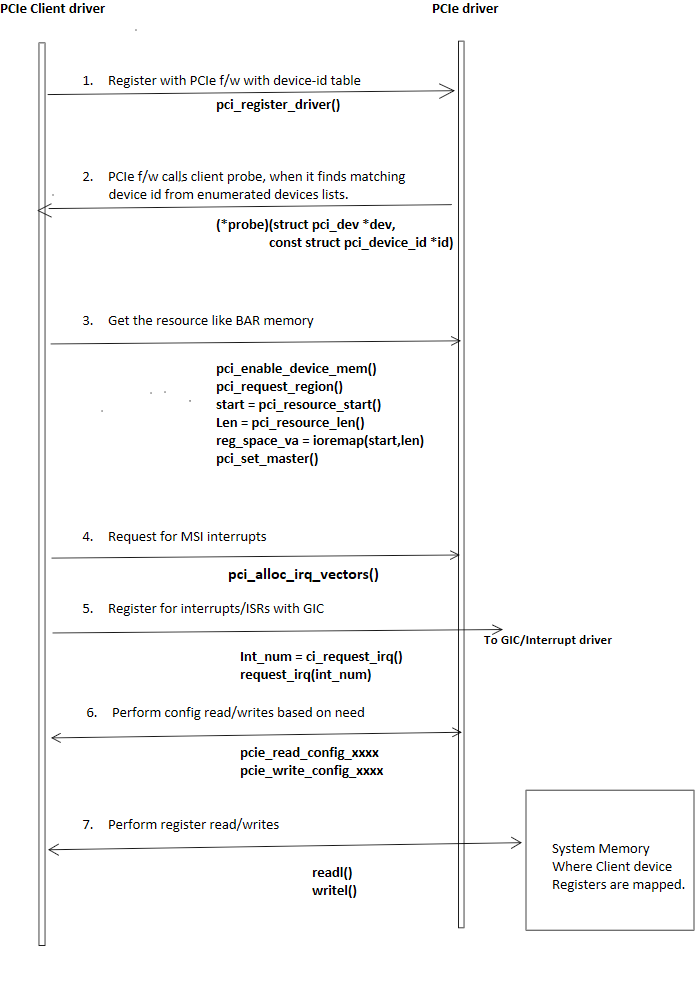
### **Client and PCI driver operation flow example**
The following figure shows the sequence that the PCIe client driver follows to configure the PCIe driver for a client.
To initiate the link training and enumeration for all endpoints, do the following:
1. To reset the QPS615 switch, toggle the RESX GPIOs for both QPS615 #1 and QPS615 #2.
2. To control the endpoint reset, trigger PERST. Both the switches share the PERST.
The devices can be attached directly to the QPS615 switch. The PCIe RC0 is attached to the WLAN endpoint. The following differences are due to the PCIe node hierarchy.
* Switch-attached devices:
* The QPS615 PCIe tree node hierarchy is statically fixed.
* All nodes for switching USP and DSP ports are created during PCIe initialization.
* One of the switch DSP ports represents WLAN.
* If you disable the WLAN node, it disables the WLAN device, but the PCIe downstream port remains enabled and returns a default maximum link width.
* Directly-attached WLAN devices:
* Disables only a single node.
* Returns the Invalid argument, when WLAN is disabled.
## **Enable NVMe through PCIe interface**
This section describes how to enable NVMe using PCIe for storage expansion. To verify if NVMe is connected over a PCIe interface, do the following:
1. To display PCIe device information, run the following command.
```text theme={null}
lspci
```
Output:
```text theme={null}
0000:00:00.0 PCI bridge: Qualcomm Device 0115
0000:01:00.0 Network controller: Qualcomm QCNFA765 Wireless Network Adapter (rev 01)
0001:00:00.0 PCI bridge: Qualcomm Device 0115
0001:01:00.0 Non-Volatile memory controller: Samsung Electronics Co Ltd NVMe SSD Controller PM9A1/PM9A3/980PRO
```
2. Locate the PCIe logs.
```text theme={null}
dmesg | grep pcie
```
Output:
```text theme={null}
[ 0.000000] Kernel command line: root=/dev/disk/by-partlabel/system rw rootwait console=ttyMSM0,115200n8
pcie_pme=nomsi net.ifnames=0 pci=noaer kpti=off kasan=off kasan.stacktrace=off swiotlb=128 earlycon reboot=panic_warm page_owner=on qcom_scm.download_mode=1 slub_debug=FZP,
zs_handle,zspage;FZPU mitigations=auto kernel.sched_pelt_multiplier=4 rcupdate.rcu_expedited=1 rcu_nocbs=0-7 no-steal-acc vfio_iommu_type1.allow_unsafe_interrupts=1 fw_devlink.strict=1
[ 3.842071] qcom-pcie 1c00000.pci: supply vdda not found, using dummy regulator
[ 3.845339] qcom-pcie 1c10000.pci: supply vdda not found, using dummy regulator
[ 3.845428] qcom-pcie 1c10000.pci: supply vddpe-3v3 not found, using dummy regulator
[ 3.845508] qcom-pcie 1c10000.pci: host bridge /pci@1c10000 ranges:
[ 3.845519] qcom-pcie 1c10000.pci: IO 0x0060200000..0x00602fffff -> 0x0000000000
[ 3.845526] qcom-pcie 1c10000.pci: MEM 0x0060300000..0x007fffffff -> 0x0060300000
[ 3.848154] qcom-pcie 1c00000.pci: supply vddpe-3v3 not found, using dummy regulator
[ 3.854556] qcom-pcie 1c00000.pci: host bridge /pci@1c00000 ranges:
[ 3.860574] qcom-pcie 1c00000.pci: IO 0x0040200000..0x00402fffff -> 0x0000000000
[ 3.867362] qcom-pcie 1c00000.pci: MEM 0x0040300000..0x005fffffff -> 0x0040300000
[ 3.963275] qcom-pcie 1c10000.pci: iATU: unroll T, 32 ob, 8 ib, align 4K, limit 1024G
[ 3.990385] qcom-pcie 1c00000.pci: iATU: unroll T, 32 ob, 8 ib, align 4K, limit 1024G
[ 4.072091] qcom-pcie 1c10000.pci: PCIe Gen.4 x2 link up
[ 4.080241] qcom-pcie 1c10000.pci: PCI host bridge to bus 0001:00
[ 4.291824] pcieport 0001:00:00.0: Adding to iommu group 9
[ 4.551677] pcieport 0001:00:00.0: PME: Signaling with IRQ 256
[ 4.572484] WARNING: CPU: 3 PID: 89 at drivers/pci/controller/dwc/pcie-qcom.c:1430 qcom_pcie_icc_update+0xf8/0x144
[ 4.595291] pc : qcom_pcie_icc_update+0xf8/0x144
[ 4.595293] lr : qcom_pcie_icc_update+0x9c/0x144
[ 4.640742] qcom_pcie_icc_update+0xf8/0x144
[ 4.640745] qcom_pcie_probe+0x234/0x30c
[ 4.988519] qcom-pcie 1c00000.pci: Phy link never came up
[ 5.302179] qcom-pcie 1c00000.pci: PCI host bridge to bus 0000:00
[ 5.372008] pcieport 0000:00:00.0: Adding to iommu group 10
[ 5.378905] pcieport 0000:00:00.0: PME: Signaling with IRQ 257
[ 11.564590] pcieport 0000:00:00.0: BAR 14: assigned [mem 0x40400000-0x405fffff]
```
3. To locate the NVMe directories, run the following command.
```text theme={null}
ls -lh /dev/nvme*
```
Output:
```text theme={null}
crw-------. 1 root root 508, 0 Jan 1 00:00 /dev/nvme0
brw-rw----. 1 root disk 259, 30 Jan 1 00:00 /dev/nvme0n1
```
## **PCIe client driver sample**
The client driver defines the `device-id` table and `pci_driver` structures, and registers with the PCIe framework. The following are a few PCIe client driver samples for reference.
* Sample data structure to hold client-specific private data.
```bash theme={null}
struct sample_driver_data {
int driver_data;
};
```
* Sample driver: You can provide data according to your driver-specific data structure.
```bash theme={null}
struct sample_driver_data info = {};
```
* Sample device ID table with the driver-specific data. The client driver registers with the `0x306` device ID.
```bash theme={null}
static const struct pci_device_id sample_pci_id_table[] = {
{ PCI_DEVICE_SUB(PCI_VENDOR_ID_QCOM, 0x0306, PCI_VENDOR_ID_QCOM, 0x010c),
.driver_data = (kernel_ulong_t) &info },
{ }
};
MODULE_DEVICE_TABLE(pci, sample_pci_id_table);
```
Note: `MODULE_DEVICE_TABLE(pci, sample_pci_id_table);` is mandatory.
* Sample `pci_driver` data structure with client driver name, `pci-id` table, and callbacks. The pointer to this structure is passed while registering with the PCI frame work.
```bash theme={null}
static struct pci_driver sample_pci_driver = {
.name = "Sample-PCI-Client-driver", /* Give the name that suites your driver description */
.id_table = sample_pci_id_table, /* pci core driver will compare from ids's supplied in this table with the enumerated endpoints */
.probe = sample_pci_probe, /* probe function is invoked by the PCI f/w when id matches with the endpoint id's */
.remove = sample_pci_remove, /* Remove function is invoked by PCI f/w when senses the attached endpoint/function is detached or down */
.driver.pm = &sample_pci_pm_ops /* pm ops that will be called from the pci core driver*/
};
```
* To register with PCI firmware, call `pci_register_driver(&sample_pci_driver)` from `module_init()`.
```bash theme={null}
module_pci_driver(sample_pci_driver);
```
## **PCIe bringup**
For information about PCIe bringup, see [PCIe-related configurations](https://docs.qualcomm.com/doc/80-80021-8/topic/pcie.html?product=895724676033554725\&facet=Interfaces\&version=2.0-rc2#pcie-software-support-feature-for-qps615__section_xbl_hhd_l1c) and [QPS615 switch support](https://docs.qualcomm.com/doc/80-80021-8/topic/pcie.html?product=895724676033554725\&facet=Interfaces\&version=2.0-rc2#pcie-software-support-feature-for-qps615__section_nmw_5jd_l1c).
## **PCIe power optimization**
PCIe defines two types of power management methods.
* Power management software that determines the power management capability of each device and manages each device individually
* System that doesn't require software intervention such as active state power management (ASPM)
During a time period when no packet is transmitted through the link, a device places the link into a power-saving state.
### **PCIe L0 link states**
PCIe power management defines the following L0 link states:
* L0: active state where all PCIe transactions and other operations are enabled
* L0s: ASPM state with low-resume latency (energy saving standby state)
### **PCIe device states**
PCIe power management defines the following device states:
* D0 (mandatory): The device is in full ON state, where there are two substates
* D0uninitialized: The function is present in the D0uninitialized state after the device comes out of reset, waiting to be enumerated and configured.
* D0active
* The function is present in the D0active state following the completion of the enumeration and configuration process.
* The function enters the D0active state when the system software enables one or more (in any combination) function parameters, such as memory space enable, I/O space enable, or BME bits.
* D1 (optional): light-sleep state
* The function can't initiate a TLP except for the PME message
* The function can't act as the target of transactions other than for configuration transactions.
* The function issues a software command to enter the D1 state by programming the PM control and status register.
* D2 (optional): deep-sleep state
* The function can't initiate a TLP except for the PME message
* The function can't act as the target of transactions other than configuration transactions.
* The function issues a software command to enter the D2 state by programming the PM control and status register.
* D3 (mandatory): device is the lowest power state, where the function must support both the D3 states
* D3hot
* The function can't initiate a TLP except for the PME message.
* The function can't act as the target of transactions other than configuration transactions.
* The function issues a software command to enter the D3hot state by programming the power state field.
* D3cold: device enters the D3cold state and power is removed; when power is restored, the device enters the D0uninitialized state.
## **PCIe verification**
For information about PCIe verification, see [PCIe-related configurations](https://docs.qualcomm.com/doc/80-80021-8/topic/pcie.html?product=895724676033554725\&facet=Interfaces\&version=2.0-rc2#pcie-software-support-feature-for-qps615__section_xbl_hhd_l1c) and [QPS615 switch support](https://docs.qualcomm.com/doc/80-80021-8/topic/pcie.html?product=895724676033554725\&facet=Interfaces\&version=2.0-rc2#pcie-software-support-feature-for-qps615__section_nmw_5jd_l1c).
## **Debug PCIe issues**
The `lspci` and `setpci` commands are native to Linux distributions. These commands have various levels of output. These commands also provide a useful point-in-time look at the capabilities and status of the different components trained on the PCI bus. Most of these capabilities are reflections of the configuration space registers required by the PCIe base specification. For more details, see [https://pcisig.com/specifications](https://pcisig.com/specifications). To view the usage instructions, run the following command.
```text theme={null}
lspci --help
```
The following features are useful in troubleshooting PCIe issues.
* Display device information
```text theme={null}
lspci
```
The following message is displayed.
```text theme={null}
0001:00:00.0 PCI bridge: Qualcomm Device 010b
0001:01:00.0 PCI bridge: Toshiba Corporation Device 0623
0001:02:01.0 PCI bridge: Toshiba Corporation Device 0623
0001:02:02.0 PCI bridge: Toshiba Corporation Device 0623
0001:02:03.0 PCI bridge: Toshiba Corporation Device 0623
0001:04:00.0 USB controller: Renesas Technology Corp. uPD720201 USB 3.0 Host Controller (rev 03)
0001:05:00.0 Ethernet controller: Toshiba Corporation Device 0220
0001:05:00.1 Ethernet controller: Toshiba Corporation Device 0220
```
* Display PCIe device and vendor IDs in the device control register.
```text theme={null}
lspci -nvmm
```
The following message is displayed.
```text theme={null}
Slot: 0001:00:00.0
Class: 0604
Vendor: 17cb
Device: 010b
DTNode: /sys/firmware/devicetree/base/soc@0/pci@1c08000/pcie@0
IOMMUGroup: 33
Slot: 0001:01:00.0
Class: 0604
Vendor: 1179
Device: 0623
DTNode: /sys/firmware/devicetree/base/soc@0/pci@1c08000/pcie@0/pcie1_bus1_dev0_fn0
IOMMUGroup: 33
Slot: 0001:02:01.0
Class: 0604
Vendor: 1179
Device: 0623
DTNode: /sys/firmware/devicetree/base/soc@0/pci@1c08000/pcie@0/pcie1_bus1_dev0_fn0/pcie1_bus2_dev1_fn0
IOMMUGroup: 33
Slot: 0001:02:02.0
Class: 0604
Vendor: 1179
Device: 0623
DTNode: /sys/firmware/devicetree/base/soc@0/pci@1c08000/pcie@0/pcie1_bus1_dev0_fn0/pcie1_bus2_dev2_fn0
IOMMUGroup: 33
Slot: 0001:02:03.0
Class: 0604
Vendor: 1179
Device: 0623
DTNode: /sys/firmware/devicetree/base/soc@0/pci@1c08000/pcie@0/pcie1_bus1_dev0_fn0/pcie1_bus2_dev3_fn0
IOMMUGroup: 33
Slot: 0001:04:00.0
Class: 0c03
Vendor: 1912
Device: 0014
Rev: 03
ProgIf: 30
DTNode: /sys/firmware/devicetree/base/soc@0/pci@1c08000/pcie@0/pcie1_bus1_dev0_fn0/pcie1_bus2_dev2_fn0/pcie1_bus4_dev0_fn0
IOMMUGroup: 33
Slot: 0001:05:00.0
Class: 0200
Vendor: 1179
Device: 0220
SVendor: 1179
SDevice: 0001
DTNode: /sys/firmware/devicetree/base/soc@0/pci@1c08000/pcie@0/pcie1_bus1_dev0_fn0/pcie1_bus2_dev3_fn0/qps615_eth0,qps615_eth0@pcie1_rp
IOMMUGroup: 33
Slot: 0001:05:00.1
Class: 0200
Vendor: 1179
Device: 0220
SVendor: 1179
SDevice: 0001
DTNode: /sys/firmware/devicetree/base/soc@0/pci@1c08000/pcie@0/pcie1_bus1_dev0_fn0/pcie1_bus2_dev3_fn0/qps615_eth1,qps615_eth1@pcie1_rp
IOMMUGroup: 33
```
For more info on PCIe debugging, see [https://www.kernel.org/doc/html/v4.17/driver-api/pci.html](https://www.kernel.org/doc/html/v4.17/driver-api/pci.html).
## **PCIe examples**
For information about the upstream device tree reference, see the following files.
* QCS6490 and QCS5430: [https://elixir.bootlin.com/linux/v7.0-rc7/source/arch/arm64/boot/dts/qcom/kodiak.dtsi](https://elixir.bootlin.com/linux/v7.0-rc7/source/arch/arm64/boot/dts/qcom/kodiak.dtsi)
* Dragonwing IQ-9075: [https://elixir.bootlin.com/linux/v7.0-rc7/source/arch/arm64/boot/dts/qcom/lemans.dtsi](https://elixir.bootlin.com/linux/v7.0-rc7/source/arch/arm64/boot/dts/qcom/lemans.dtsi)
* Dragonwing IQ-615: [https://git.kernel.org/pub/scm/linux/kernel/git/qcom/linux.git/tree/arch/arm64/boot/dts/qcom/qcs615.dtsi?h=arm64-for-6.16](https://git.kernel.org/pub/scm/linux/kernel/git/qcom/linux.git/tree/arch/arm64/boot/dts/qcom/qcs615.dtsi?h=arm64-for-6.16)
* [https://git.kernel.org/pub/scm/linux/kernel/git/torvalds/linux.git/tree/drivers/pci/controller/dwc/pcie-qcom.c?h=v6.8-rc6#n1634](https://git.kernel.org/pub/scm/linux/kernel/git/torvalds/linux.git/tree/drivers/pci/controller/dwc/pcie-qcom.c?h=v6.8-rc6#n1634)
For information about device-tree node for the Qualcomm Linux hardware SoCs, see the following DTSI files.
* QCS6490 and QCS5430: [https://elixir.bootlin.com/linux/v7.0-rc7/source/arch/arm64/boot/dts/qcom/kodiak.dtsi](https://elixir.bootlin.com/linux/v7.0-rc7/source/arch/arm64/boot/dts/qcom/kodiak.dtsi)
* Dragonwing IQ-9075: [https://elixir.bootlin.com/linux/v7.0-rc7/source/arch/arm64/boot/dts/qcom/lemans.dtsi](https://elixir.bootlin.com/linux/v7.0-rc7/source/arch/arm64/boot/dts/qcom/lemans.dtsi)
* Dragonwing IQ-615: [https://git.kernel.org/pub/scm/linux/kernel/git/qcom/linux.git/tree/arch/arm64/boot/dts/qcom/qcs615.dtsi?h=arm64-for-6.16](https://git.kernel.org/pub/scm/linux/kernel/git/qcom/linux.git/tree/arch/arm64/boot/dts/qcom/qcs615.dtsi?h=arm64-for-6.16)
### **Client and PCI driver operation flow example**
The following figure shows the sequence that the PCIe client driver follows to configure the PCIe driver for a client.
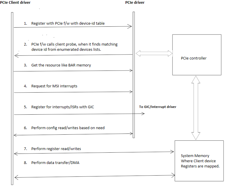 ### **Client and PCI driver high-level call flow example**
The following figure shows the high-level call flow and call details between the PCIe client driver and PCIe driver.
### **Client and PCI driver high-level call flow example**
The following figure shows the high-level call flow and call details between the PCIe client driver and PCIe driver.