> ## Documentation Index
> Fetch the complete documentation index at: https://dragonwingdocs.qualcomm.com/llms.txt
> Use this file to discover all available pages before exploring further.
# 外设接口概述
Qualcomm® Linux® 接口指南介绍了片上系统(SoC)中使用的低速和高速输入/输出(I/O)外设接口子系统。
* 低速 I/O 接口的工作频率低于 SoC 中的高速接口。Qualcomm 通用外设(QUP)v3 串行引擎是一个硬件核心,支持以下低速外设接口:
* 通用异步收发器([UART](https://dragonwingdocs.qualcomm.com/System/Interfaces/uart))
* 串行外设接口([SPI](https://dragonwingdocs.qualcomm.com/System/Interfaces/spi))
* 互联集成电路([I2C](https://dragonwingdocs.qualcomm.com/System/Interfaces/i2-c))
* 改进型互联集成电路([I3C](https://dragonwingdocs.qualcomm.com/System/Interfaces/i3-c))
这些低速接口与低速外设通信,例如传感器接口设备、Bluetooth® 无线技术设备、显示或触摸接口设备。
* 高速 I/O 接口包括以下外设接口:
* 外设组件互连高速通道([PCIe](https://dragonwingdocs.qualcomm.com/System/Interfaces/pcie))
* 通用串行总线([USB](https://dragonwingdocs.qualcomm.com/System/Interfaces/usb))
高速 I/O 接口用于连接高速设备,例如固态硬盘、网卡、外部显卡。
## 外设接口软件栈
下图显示了外设接口的软件栈。
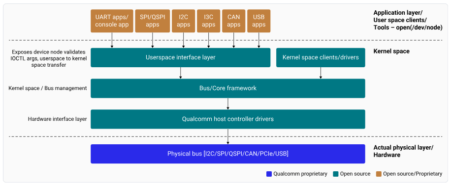 **图:外设接口软件栈高层结构(高层视图)**
**从应用程序到 QUP GENI 硬件(Linux 高层流程)**
在 Linux 中,应用程序通过内核提供的标准用户空间接口(例如 `/dev` 节点或子系统 API)与外设通信。流程如下:
1. 应用层
* 应用程序使用标准用户空间接口发出请求。
* 请求通过系统调用进入内核。
2. 内核核心框架
* 内核将请求路由到相关的子系统,例如:
* I2C
* SPI
* I3C
* TTY
* 该子系统执行以下功能:
* 提供协议感知的抽象
* 管理同步和并发
* 集成电源管理钩子
* 为客户端提供统一的编程接口
3. 协议控制器驱动程序
* 核心框架调用协议控制器驱动程序。
* 驱动程序将框架级操作转换为硬件特定的命令。
4. QUPv3 GENI 串行引擎(Qualcomm 平台)
* 控制器驱动程序对 QUPv3 GENI 串行引擎进行编程。
* GENI 使用以下方式实现所选协议(I2C、SPI、I3C 或 UART):
* 已配置的传输模式
* 协议固件
5. GENI 硬件执行
* 执行寄存器级操作。
* 在系统与外部设备之间移动数据。
在整个过程中,内核框架始终控制以下内容:
* 驱动程序和设备生命周期管理
* 并发处理
* 整个软件栈的电源状态协调
下图显示了从应用程序到 QUP-GENI 硬件的 Linux 流程。
**图:外设接口软件栈高层结构(高层视图)**
**从应用程序到 QUP GENI 硬件(Linux 高层流程)**
在 Linux 中,应用程序通过内核提供的标准用户空间接口(例如 `/dev` 节点或子系统 API)与外设通信。流程如下:
1. 应用层
* 应用程序使用标准用户空间接口发出请求。
* 请求通过系统调用进入内核。
2. 内核核心框架
* 内核将请求路由到相关的子系统,例如:
* I2C
* SPI
* I3C
* TTY
* 该子系统执行以下功能:
* 提供协议感知的抽象
* 管理同步和并发
* 集成电源管理钩子
* 为客户端提供统一的编程接口
3. 协议控制器驱动程序
* 核心框架调用协议控制器驱动程序。
* 驱动程序将框架级操作转换为硬件特定的命令。
4. QUPv3 GENI 串行引擎(Qualcomm 平台)
* 控制器驱动程序对 QUPv3 GENI 串行引擎进行编程。
* GENI 使用以下方式实现所选协议(I2C、SPI、I3C 或 UART):
* 已配置的传输模式
* 协议固件
5. GENI 硬件执行
* 执行寄存器级操作。
* 在系统与外部设备之间移动数据。
在整个过程中,内核框架始终控制以下内容:
* 驱动程序和设备生命周期管理
* 并发处理
* 整个软件栈的电源状态协调
下图显示了从应用程序到 QUP-GENI 硬件的 Linux 流程。
 **图:外设接口软件栈高层结构(低层视图)**
## QUP v3
Qualcomm 使用 QUP v3——一种高度灵活且可编程的硬件——来支持各种串行接口。有关 QUP v3 的更多信息,请参阅以下资源:
* [QUP v3 概述](https://dragonwingdocs.qualcomm.com/System/Interfaces/references#qup-v3-overview)
* [QUP v3 支持的传输模式](https://dragonwingdocs.qualcomm.com/System/Interfaces/references#supported-transfer-modes-in-qup-v3)
* [QUP v3 访问控制自定义](https://dragonwingdocs.qualcomm.com/System/Interfaces/references#qup-v3-access-control-customization)
* [QUP v3 固件状态验证](https://dragonwingdocs.qualcomm.com/System/Interfaces/references#qup-v3-firmware-status-verification)
**注意**
* boot 和 aDSP 子系统的源代码面向具有授权访问权限的许可开发人员提供。
* 请参阅 Qualcomm Linux 支持的[硬件 SoC](https://dragonwingdocs.qualcomm.com/Hardware-SoCs)。
本指南是您了解如何启用低速和高速 I/O 接口以及进行配置更改的主要参考资源。
**注意**
在本指南中,`` 指 QCS6490、QCS5430、Qualcomm Dragonwing™ IQ-9075、Qualcomm Dragonwing™ IQ-8275 或 Qualcomm Dragonwing™ IQ-615。例如,对于 `arch/arm64/boot/dts/qcom/.dts`,相应的设备树源(DTS)文件位于 [https://github.com/torvalds/linux/blob/master/arch/arm64/boot/dts/qcom/qcs6490-rb3gen2.dts](https://github.com/torvalds/linux/blob/master/arch/arm64/boot/dts/qcom/qcs6490-rb3gen2.dts) 或 [https://github.com/torvalds/linux/blob/master/arch/arm64/boot/dts/qcom/sa8775p.dtsi](https://github.com/torvalds/linux/blob/master/arch/arm64/boot/dts/qcom/sa8775p.dtsi) 或 [https://git.kernel.org/pub/scm/linux/kernel/git/qcom/linux.git/tree/arch/arm64/boot/dts/qcom/qcs615.dtsi?h=arm64-for-6.16](https://git.kernel.org/pub/scm/linux/kernel/git/qcom/linux.git/tree/arch/arm64/boot/dts/qcom/qcs615.dtsi?h=arm64-for-6.16)。
**图:外设接口软件栈高层结构(低层视图)**
## QUP v3
Qualcomm 使用 QUP v3——一种高度灵活且可编程的硬件——来支持各种串行接口。有关 QUP v3 的更多信息,请参阅以下资源:
* [QUP v3 概述](https://dragonwingdocs.qualcomm.com/System/Interfaces/references#qup-v3-overview)
* [QUP v3 支持的传输模式](https://dragonwingdocs.qualcomm.com/System/Interfaces/references#supported-transfer-modes-in-qup-v3)
* [QUP v3 访问控制自定义](https://dragonwingdocs.qualcomm.com/System/Interfaces/references#qup-v3-access-control-customization)
* [QUP v3 固件状态验证](https://dragonwingdocs.qualcomm.com/System/Interfaces/references#qup-v3-firmware-status-verification)
**注意**
* boot 和 aDSP 子系统的源代码面向具有授权访问权限的许可开发人员提供。
* 请参阅 Qualcomm Linux 支持的[硬件 SoC](https://dragonwingdocs.qualcomm.com/Hardware-SoCs)。
本指南是您了解如何启用低速和高速 I/O 接口以及进行配置更改的主要参考资源。
**注意**
在本指南中,`` 指 QCS6490、QCS5430、Qualcomm Dragonwing™ IQ-9075、Qualcomm Dragonwing™ IQ-8275 或 Qualcomm Dragonwing™ IQ-615。例如,对于 `arch/arm64/boot/dts/qcom/.dts`,相应的设备树源(DTS)文件位于 [https://github.com/torvalds/linux/blob/master/arch/arm64/boot/dts/qcom/qcs6490-rb3gen2.dts](https://github.com/torvalds/linux/blob/master/arch/arm64/boot/dts/qcom/qcs6490-rb3gen2.dts) 或 [https://github.com/torvalds/linux/blob/master/arch/arm64/boot/dts/qcom/sa8775p.dtsi](https://github.com/torvalds/linux/blob/master/arch/arm64/boot/dts/qcom/sa8775p.dtsi) 或 [https://git.kernel.org/pub/scm/linux/kernel/git/qcom/linux.git/tree/arch/arm64/boot/dts/qcom/qcs615.dtsi?h=arm64-for-6.16](https://git.kernel.org/pub/scm/linux/kernel/git/qcom/linux.git/tree/arch/arm64/boot/dts/qcom/qcs615.dtsi?h=arm64-for-6.16)。