

This section describes the hardware and software architecture block diagram of RTSS.
RTSS hardware architecture
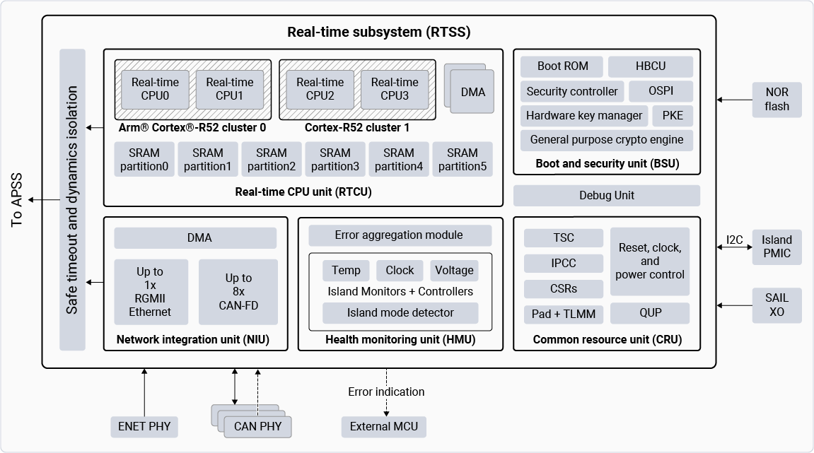
The following diagram shows the RTSS architecture, highlighting its key functional units and their connections. This architecture supports robust real-time performance, secure booting, fault monitoring, and flexible networking.
rtss_hardware_architecture.png
RTSS hardware architecture

RTSS software architecture


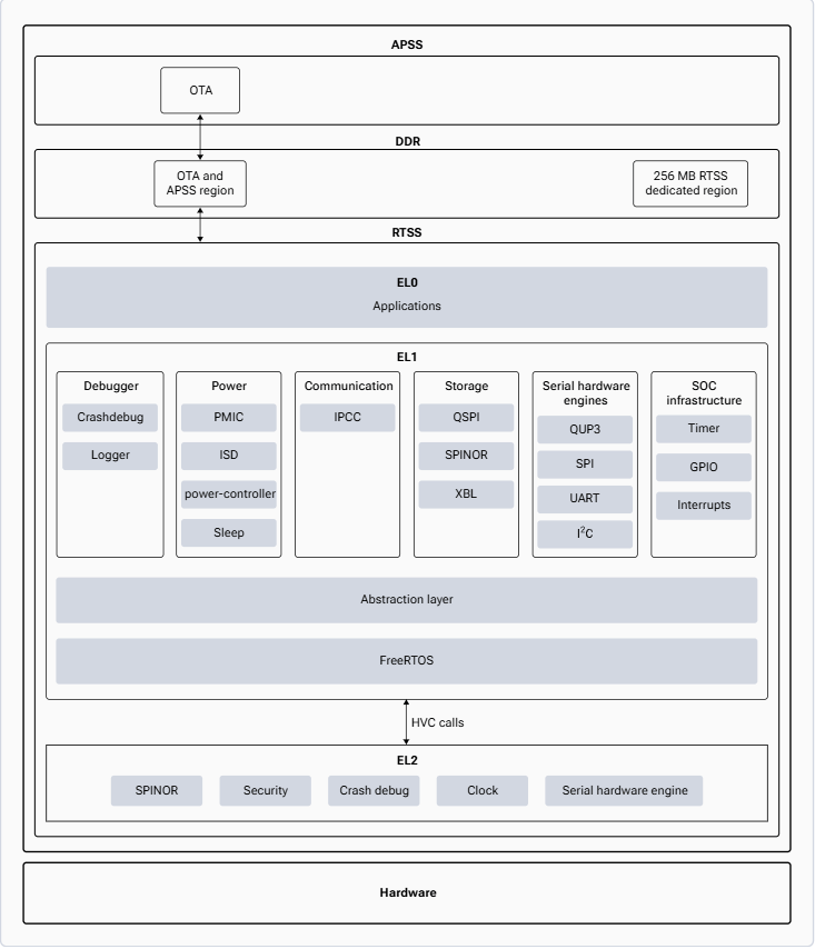
The following diagram shows a modular embedded system architecture designed for safety-critical and sensor-driven applications.
rtss_software_architecture.png
RTSS software architecture The following are the key components: Power Management Integrated Circuit (PMIC) PMIC regulates and distributes the power to various components of a device such as CPU and memory. The PMIC driver does the following:
  • Voltage regulation, which ensures that each component receives the correct operating voltage.
  • Power sequencing, which controls the order in which different components of the device power on or off, ensuring seamless operation.
Island State Detector (ISD) ISD does the following:
  • Moves the RTSS into the Island state during the following stages:
    • Chip cold boot
    • RTSS Low-Power mode
    • APSS and RTSS crashes/faults
  • Detects errors and initiates the Island state during cold boot and fault conditions.
  • Handles reset requests from APSS.
  • Notifies the critical RTSS errors to APSS that may require a SoC reset or entry into the Emergency Download (EDL) mode.
Interprocess Communication Controller (IPCC) IPCC does the following:
  • Uses signals delivered as interrupts for interprocess communication.
  • Follows a star topology, requiring only one interrupt request (IRQ) input wire per core per protocol.
  • Acts as a centralized block for managing IPC interrupts at the SoC level.
  • Enables communication and synchronization between multiple processors using message queues, shared memory, signals, and semaphores.
Serial peripheral interface NOR (SPINOR) flash memory The system includes a single SPINOR controller, shared by all users across Exception level 1 (EL1) and Exception level 2 (EL2). The EL1 SPINOR driver:
  • Communicates with the EL2 driver using trap system calls.
  • Handles context switching and data sharing between EL1 and EL2, abstracting these details from client applications.
The EL2 SPINOR driver:
  • Holds privileged access to the SPINOR hardware.
  • Manages all client requests from both EL1 and EL2.
  • Coordinates operations and ensures secure access control between execution levels.
Serial peripheral interface (SPI) SPI has a 4-wire synchronous serial interface for data communication. Data communication is enabled with a chip select (CS) wire, controller data output and target data input for serial data output, controller data input and target data output for serial data input, and serial clock (CLOCK) synchronizes data transmission. SPI is used to connect with CAN transceiver. Universal Asynchronous Receiver Transmitter (UART) The UART driver supports communication between RTSS, both the debug port, and VIP SoC. It uses the RTSS QUP hardware, which operates in the Direct memory access (DMA) mode and can only access QUP RAM. Therefore, all the UART buffers must be allocated in QUP RAM. Inter-integrated circuit (I2C) The I2C protocol enables controller-target communication over a shared bus. The I2C controller initiates data transfers to read from or write to the connected target devices. The PMIC driver uses the I2C driver to communicate with the target devices on the I2C bus. The PMIC clients act as controllers, interacting with external targets using the I2C interface. General-purpose timer (GPT) The GPT driver provides services and configuration parameters for starting and stopping the hardware timers, getting timer values, controlling time triggered interrupt notifications, controlling time triggered wakeup interrupts if supported by hardware. The tick duration of each timer channel depends on its specific configuration, the system clock, and clock tree settings. General-purpose input/output (GPIO) The TLMM driver provides interfaces to configure, read input/output values and write output value to a GPIO. A GPIO is configured as input/output or as a special function GPIO. The TLMM driver also supports receiving interrupts from GPIO. Interrupts can be generated as level triggered, rising edge, falling edge or dual edge triggered. Generic interrupt controller (GIC) The GIC receives interrupts from system sources like bus exceptions and from private CPU peripherals such as timers and power control units. All interrupts are routed to the top of the GIC using SPI and PPI input signals. Interrupts are then delivered to CPU cores through the internal GIC CPU interface using the irq_n and fiq_n signals. Hypervisor call (HVC) HVC calls are used when EL1 performs privileged operations in EL2. Since EL1 doesn’t have access to system registers or memory regions that are reserved for EL2, HVC calls communicate between EL1 and EL2 to execute the privileged tasks.

Next steps